お問い合わせカート
Introduction
About E&R
Milestone
Our Vision
Core Tech
Global location
Organization
Safety Regulation
Contact Us
TGV workshop
Laser process development
Small scale production
Plasma treatment
EMC residue removal
Copper oxide removal
Silicon oxide deposition
Chip stress relief
Laser micromachining, Silicon
Thin wafer dicing
Wafer grooving
Laser micromachining, Glass
TGV, through glass via
Glass cavity/frame
Glass cutting
Laser micromachining, EMC
Fan-out wafer drilling/pattering
Fan-in wafer dicing
Laser micromachining, SiC
SiC wafer dicing
繁
En
简
繁
|
En
|
简
お問い合わせカート
(
)
お問い合わせ
ホームページ
Products
Laser Solution
Micromachining
Wafer & Frame Form
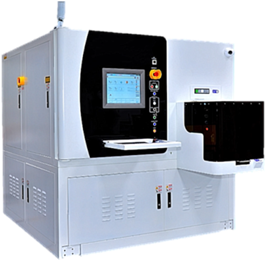
WS Series
数量 :
見積をする